

I am in Bay Area, USA for 2 weeks which will take me to Silicon Valley, Redmond (WA) and Los Angeles (for Microsoft PDC ’08). Sunday evening I went along with my cousin who lives here to Fremont Temple. This is a well maintained and spacious (considering it is outside India) temple and I was impressed by the newly build area for the South Indian gods.
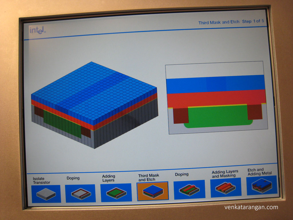
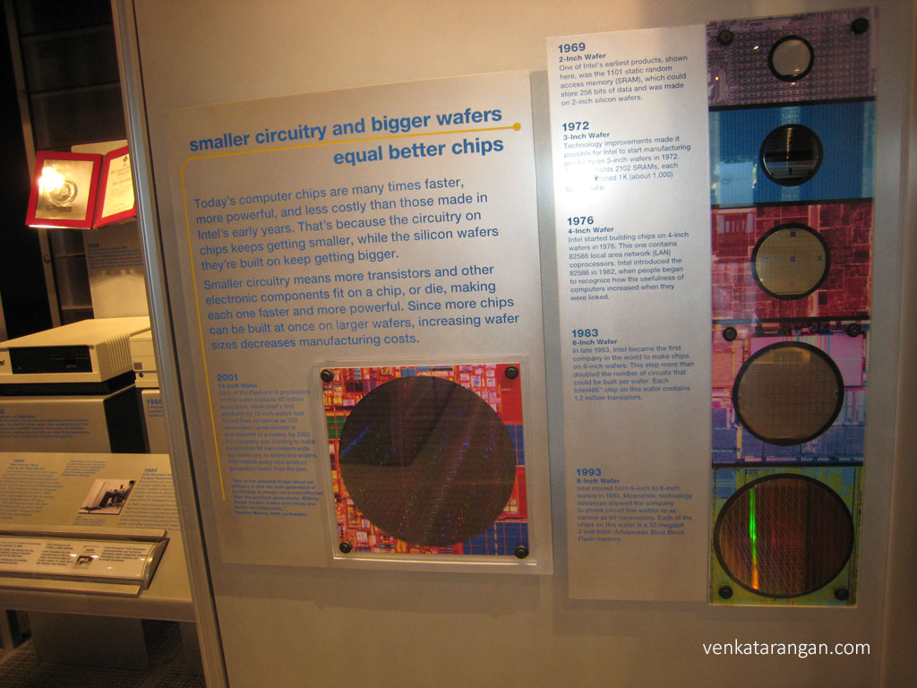
On Monday morning I went to the Intel Museum in their campus in Santa Clara (CA). The museum covers about the history of Intel from memory chips, 4004 to the latest chips; chip fabrication process and basics of silicon, etc. The self-visit doesn’t take more than 30 minutes and I will recommend visiting this only if you happen to be in the Silicon Valley area. Not worth travelling from anywhere far for this. I was told most of this is available online on their website as well.


Seeing the Intel 386 PC on display brought old memories for me. I started learning and doing extensive programming first on this PC – a 386SX (without the math co-processor) computer from Wipro during my school days. It is on this PC I learned my first business programming language – FoxBase and then Clipper. It is amazing the progress we have had in terms of speed and features over the last 23 years – unbelievable.

Discover more from Mangoidiots
Subscribe to get the latest posts sent to your email.